IBM Announces 1 nm Chip Breakthrough
The new nanostack architecture enables 0.7 nm chip architecture and a 50% performance gain over 2 nm chips, according to projections

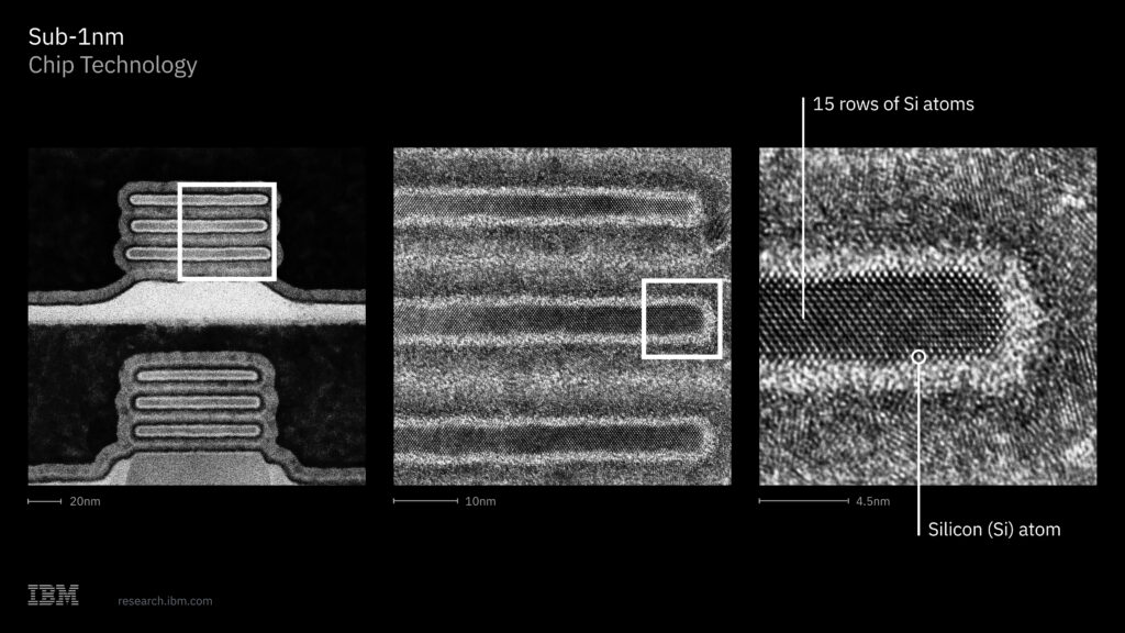
IBM announced last week it has broken through a new semiconductor scaling barrier with the introduction of the world’s first sub-1 nanometer (nm) chip technology, dubbed “nanostack” architecture.
The innovation has enabled a 0.7 nm chip architecture that IBM says can squeeze nearly 100 billion transistors onto a chip the size of a fingernail, thanks to a new way of arranging those atomic-scale components.
“With this week’s announcement, the introduction of nanostack, it will be for the first time in our industry we are able to stack and stagger transistors in the vertical direction,” Hueming Bu, VP of silicon technology R&D at IBM, explained during a press briefing introducing the breakthrough.
According to IBM projections, this approach will result in as much as a 50% performance gain over today’s best 2 nm chips, 40% improvement in SRAM density and up to 70% greater energy efficiency.
These improvements will be especially welcome in compute-heavy AI use cases. “This achievement of 40% (improved SRAM density) will eventually industrialize itself in AI workflows which require higher bandwidth and high efficiency,” said Jay Gambetta, director of IBM Research and IBM Fellow.
Enter the Angstrom
“IBM’s latest chip breakthrough marks a landmark moment in computing, pushing technology beyond the nanometer era to the scale of atoms,” said Jay Gambetta, director of IBM Research and IBM Fellow.
With that, the technology is increasingly being described in terms more commonly used by physicists and chemists, as the angstrom (Å) enters the hardware lexicon. 1 Å equals 0.1 nm, while a silicon atom has a diameter of about 2 Å.
IBM expects nanostack architecture to make it into mass production as early as five years from now, a path enabled by several interlocking innovations feeding into nanostack architecture.
“With our new nanostack architecture, we’re not just making smaller transistors; we’re reinventing how chips are built to deliver dramatically more power and energy efficiency,” Gambetta said.
These improvements will be especially welcome in compute-heavy AI use cases. “This achievement of 40% (improved SRAM density) will eventually industrialize itself in AI workflows which require higher bandwidth and high efficiency,” he said.
Building on the Nanosheet Breakthrough
Nanostack builds on the IBM-developed “nanosheet” architecture, which enabled the breakthrough to 2 nm scale announced in 2021, an advance that put 50 billion transistors on a fingernail-sized chip. To combat the electron leakage that increases at such scale, nanosheet employs a “gate-all-around” architecture, which completely wraps around the channel (conductive path) to better control the flow of electricity, Bu explained.
Also key to nanostack architecture is an innovation called dielectric bonding. This technology bonds transistors at atomic dimensions via a non-conductive, ultra-thin insulating layer—the dielectric layer. Bu said that because the transistors are built separately before bonding, each can be developed with different materials and independently optimized.
‘Almost a Magic’
Bu turned to non-scientific terminology to describe the staggeringly minuscule scale that made IBM’s latest chip breakthrough possible. Once it achieved 3 nm technology, IBM entered a domain where “semiconductor manufacturing is almost a magic,” Bu said, because that atom-by-atom engineering scale is where the strange laws of quantum mechanics start taking effect.
This means engineers have to address challenges like “quantum tunneling,” where electrons pass through barriers they shouldn’t be able to cross under the laws of classical physics. The dielectric innovations in the insulating layers surrounding the nanosheets are designed to minimize such disruption, Bu explained.
Dielectric bonding is key to IBM’s chip scaling aspirations, and a reason “why (nanostack) is not a one-time innovation,” Bu said. The new platform, he continued, will drive several generations of chip technology—from ”7 angstrom, 5 angstrom, 3 angstrom, all the way to 1 angstrom.”